Hello,
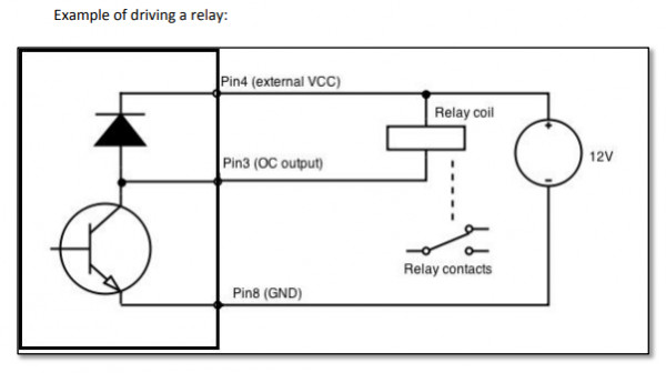
To be more clear I'd like you to look at the picture below, as it shows some approximation of internal details. Since internal circuitry voltage levels are lower than the actual allowed maximum voltage by the transistor, it has to be supplied from the external source. Actual values may differ, but, for example, a 5V signal from the integrated circuit applied to the base of the transistor can drive the load, for example a relay, which requires 12V supply. The idea is that transistor in open collector configuration works as a switch. When no base voltage is applied its state is off. In order to have the drive capacity, there needs to be a voltage drop upon its terminals, thus, the need for Pin 4 as a stable reference and pin 3 for output state control.
Best regards,
